
Nvidia quietly cuts Vera Rubin's memory and NVLink bandwidth specs
Nvidia lowered its published HBM4 and NVLink 6 bandwidth figures for Vera Rubin without any announcement. The biggest hit lands on the eight-GPU HGX Rubin NVL8.
 Merhabyte Newsdesk · · 4 min read
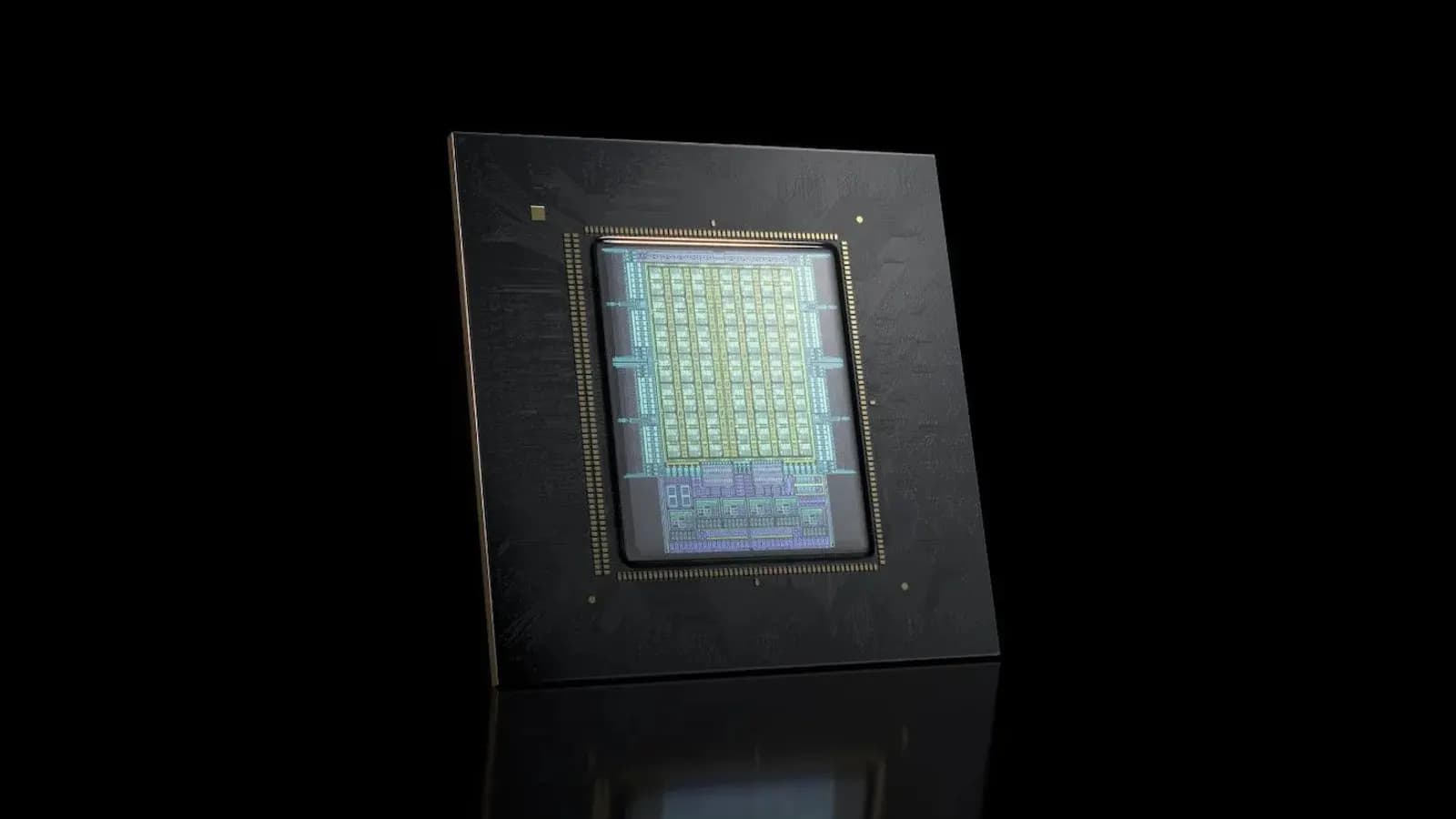
Nvidia has lowered the memory and interconnect bandwidth figures it publishes for the Vera Rubin platform without saying anything. On the Vera Rubin NVL72 product page, each Rubin GPU's HBM4 bandwidth is now listed as 19.2 TB/s instead of 22 TB/s, and NVLink 6 bandwidth as 3 TB/s instead of 3.6 TB/s. That works out to a drop of roughly 13 percent for HBM4 and roughly 17 percent for NVLink.
Memory capacity stays at 288 GB, and the 50 PFLOPS headline figure for sparse NVFP4 inference is unchanged. At rack scale, however, total memory bandwidth fell from 1,580 TB/s to 1,400 TB/s, and total NVLink bandwidth from 260 TB/s to 216 TB/s. The two-GPU Vera Rubin Superchip went from 44 TB/s to 38.5 TB/s.
The change was made on product pages, with no announcement
The revision came to light when Nvidia's documentation was compared against a copy saved in June 2026. Wayback Machine archives show the edit was made between September 1 and 11, meaning the new numbers had been on the site for at least six weeks before anyone wrote about them.
The timing is notable. In its August second-quarter results, Nvidia said Vera Rubin racks were running at partners including CoreWeave, Google Cloud and Microsoft Azure. The autumn production shipments promised in May are also due to begin around now. That suggests the new values describe hardware coming off the line rather than a distant target.
HGX Rubin NVL8 takes the biggest loss
The reductions are not proportional across configurations. The HGX Rubin NVL8, Nvidia's standard eight-GPU server board, was hit hardest. System-wide HBM4 capacity fell from 2.3 TB to 2 TB, and bandwidth from 176 TB/s to 130 TB/s, a 26 percent loss. NVLink Switch bandwidth dropped from 28.8 TB/s to 24 TB/s. Dense training performance slipped from 280 to 270 PFLOPS in NVFP4 and from 140 to 130 PFLOPS in FP8.
The only line item that rose is scale-out network bandwidth, which is up 12.5 percent in most configurations; Nvidia did not explain why.
The numbers also do not fully line up. The per-GPU table still shows 288 GB, 22 TB/s and 3.6 TB/s of NVLink, which does not match the new system totals printed next to it. Nvidia's July presentation of the Rubin architecture likewise continues to describe 22 TB/s. Divide the new totals by eight GPUs and you get roughly 16.25 TB/s and roughly 250 GB per GPU. That could point either to eight smaller HBM4 stacks running slightly below 8 Gbps per pin or to one stack per GPU being disabled. Nvidia is known to have used a similar approach on the 80 GB H100, but the company has not said which route it took.
Why the HBM4 target may have slipped
The HBM4 standard JEDEC published in April 2025 defines up to 8 Gb/s per pin and 2 TB/s per stack over a 2,048-bit interface. Nvidia's target was far above that. According to an earlier report, Rubin's per-GPU bandwidth goal was 13 TB/s at GTC 2025, rose to 20.5 TB/s in September, and reached 22 TB/s at CES 2026. The same report cited a note saying SK hynix and Samsung were struggling to hit the final figure and that first shipments were expected to land around 20 TB/s.
Market researchers predicted in September 2025 that Nvidia was asking suppliers for 10 Gbps per pin and might back off the increase if volume fell short or costs climbed, or might split platform products into tiers. In January, demand was reported to have exceeded 11 Gbps, with all three memory makers going back to redesign. Nvidia, for its part, had said its HBM4 partners were on track for production shipments. SK hynix was first to finish HBM4 development, and Samsung began shipping in February at 11.7 Gbps. Even so, the revised table looks like the fallback scenario: a lower ceiling plus a downgraded HGX tier. It can be read as Nvidia prioritizing delivery to customers over chasing a perfect memory target.
On paper, AMD pulls ahead
The competitive picture has changed, at least on paper. AMD's Instinct MI455X offers 432 GB across 12 HBM4 stacks and 23.3 TB/s, needing only about 7.6 Gbps per pin to do it, below the JEDEC baseline. AMD gets its bandwidth from width rather than speed, so it never needed above-standard memory.
When AMD unveiled Helios in July 2026, it claimed 6 percent more HBM bandwidth than Vera Rubin NVL72's published figure. Against the revised 1,400 TB/s, Helios's 1.67 PB/s is roughly 19 percent ahead. On scale-up bandwidth, traditionally an Nvidia strength, the two were level at 260 TB/s per rack; the gap is now about one-fifth in AMD's favor. The scale-out increase trims AMD's claimed 50 percent advantage to roughly a third. None of these figures has been confirmed by independent testing.
For inference workloads, bandwidth matters more than FLOPS. In its July architecture document, Nvidia engineers argue that the decode phase is bound by the memory subsystem and that what counts is how efficiently the cores use memory rather than peak figures. The marketing language has not changed: the NVL72 page maintains its promise of up to 10 times more tokens per megawatt and one-tenth the cost per million tokens versus GB200 NVL72, footnoted as subject to change.
Comments
No comments yet. Be the first to comment.