Tesla Roadmap: SI6 Chip to Deliver 80x HW4 Compute
Tesla's updated chip roadmap says its sixth-generation inference chip will offer 80 times the compute of today's fourth-generation part. The Dojo D3 trainer moves to chiplets with stacked HBM.
 Merhabyte Newsdesk · · 3 min read
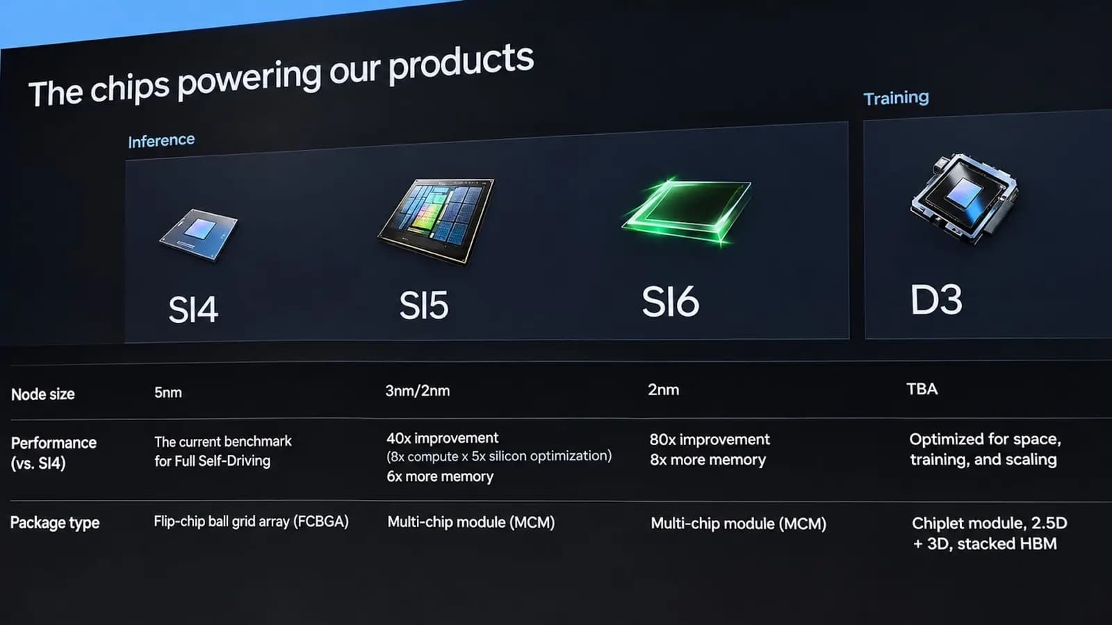
Tesla has shared an updated roadmap for its AI accelerators, offering a look at where its chip development is heading. According to the presentation, the sixth-generation inference accelerator is expected to deliver 80 times the compute of the current fourth-generation chip. On the training side, the D3 accelerator will drop the SRAM-centric architecture in favor of a multi-chiplet design with stacked HBM memory.
One notable detail is the naming. Tesla now refers to its accelerators with the prefix SI, derived from superintelligence, rather than AI. The chips previously known as AI4, AI5 and AI6 appear in this roadmap as SI4, SI5 and SI6. Elon Musk has reportedly confirmed recently that SpaceXAI will be renamed SpaceXSI for the same reason. The details come from a slide said to belong to Tesla, so some of the information is speculative.
Dojo D3 returns with a different architecture
The most intriguing part of the roadmap is the return of the Dojo training accelerator. Musk cancelled the wafer-scale Dojo project in August 2025, and in August 2026 said SpaceX and xAI would use only Nvidia hardware in their data centers, both on the ground and in space. Even so, the third-generation Dojo is coming back with a design that differs markedly from the first two generations.
Tesla describes D3 as a chiplet-based design that combines 2.5D and 3D packaging with stacked HBM. The original Dojo D1 relied on wafer-scale packaging, linking 25 D1 processors and using distributed on-chip SRAM, with roughly 11 GB of SRAM per wafer. The move to HBM suggests Tesla wants to expand memory capacity substantially, since modern AI models need very large amounts of memory for parameters, activations and intermediate data. HBM makes scaling easier but brings different trade-offs in latency, bandwidth, packaging and power consumption.
It is unclear whether wafer-scale integration has been abandoned entirely. Stacking HBM on top of logic dies raises design complexity, cooling challenges, manufacturing difficulty and cost, which makes wafer-scale scaling less likely for D3. Tesla has not yet disclosed D3's performance, memory capacity, manufacturing process or schedule. The company says only that the accelerator will be optimized for space, training and scaling, which may point to a conventional accelerator architecture and, for at least some versions, possibly a radiation-hardened design.
An 80x performance target for SI6
The roadmap also gives approximate compute figures for the sixth-generation inference processor, SI6. Tesla says SI6 will offer 80 times the compute and 9 times the memory of HW4. Depending on how HW4's performance is measured, that works out to roughly 17,280 to 46,080 TOPS, or 17.28 to 46.08 POPS. The data formats SI6 will support are unknown, and the figures are estimates.
For comparison, Nvidia's Rubin GPU delivers 50 NVFP4 PFLOPS for inference, and 35 NVFP4 PFLOPS plus 17.5 FP8/FP6 PFLOPS for training. Rubin is reaching customers today, while SI6 is expected to arrive in the 2029-2030 timeframe.
Current chips and the transition table
The fourth-generation inference processor used in Tesla vehicles today, known first as HW4, then AI4 and now SI4, is built by Samsung Foundry and uses conventional FCBGA packaging. Because of an error on the slide, the chip is claimed to be made on a 5nm-class process, while the table lists it as Samsung 7nm. Its memory is estimated to be 16 GB of GDDR6. Tesla presents this processor as the current reference point for its Full Self-Driving technology.
Other details in the table show the older HW3 chip on Samsung's 14nm process with 8 GB of LPDDR4 memory, marked as a legacy generation. SI5 is listed on TSMC 3nm or Samsung 2nm, with a multi-chip module (MCM) architecture and at a stage approaching production. SI6 is shown on a 2nm-class process, also with an MCM architecture, and still in development. Memory for SI5 (GDDR6/GDDR7) and SI6 (GDDR7) is marked with question marks, so those details are not firm.
Comments
No comments yet. Be the first to comment.